hongyavision HYWS-SGT0204S
RTL8372-based 4×2.5G + 2×SFP+ unmanaged switch.
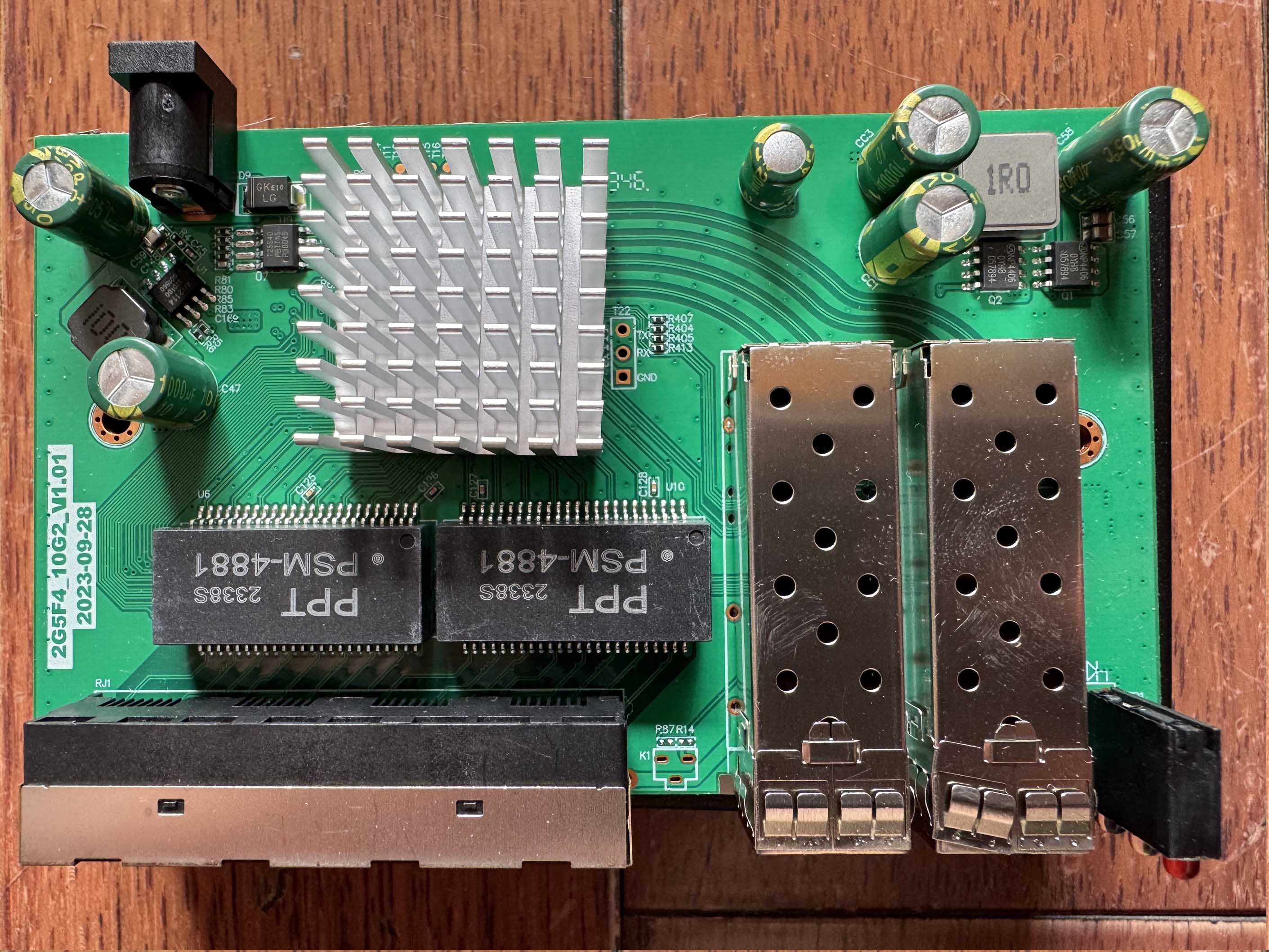
Also marked on the PCB as `2G5F4_10G2_V1.01`.
Stock firmware runs a factory test console on UART at 9600 baud 8N1 (banner
`RTL8371B start`, prompt `RTL8371B:`). There is no management CLI and no Web
interface.
Using SPI clamp in-board is the only method for initial installation and update.
Erase the whole chip and verify the write (`flashrom -v`) before powering the
board, so an incomplete write is caught before the board is powered up.
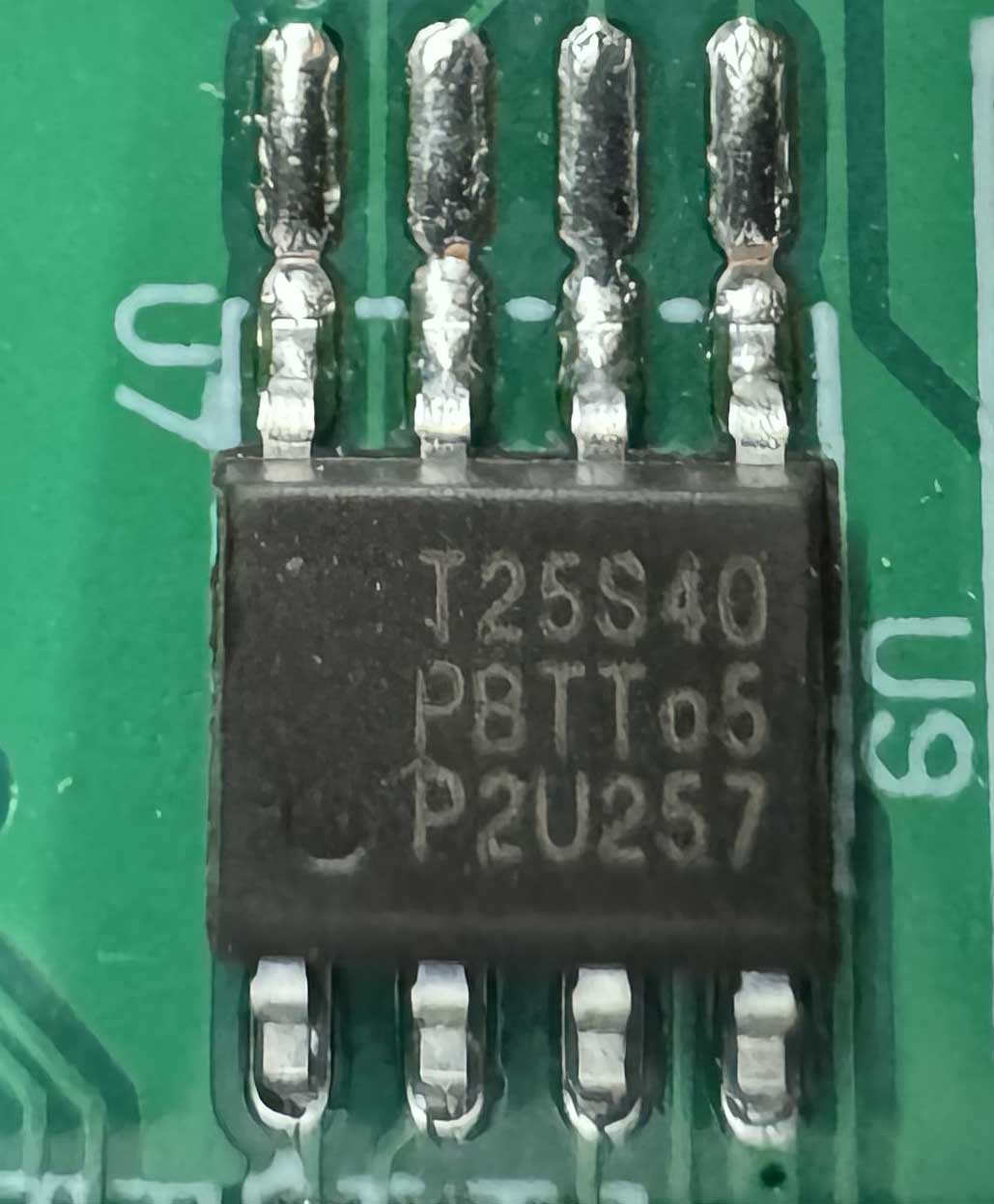
Stock flash chip is 512 KB (Bright Moon `T25S40`, 4 Mbit, SOP-8), which the
RTLPlayground image fills exactly.
### Label specifications
- **Manufacturer**: hongyavision
- **Model**: HYWS-SGT0204S
- **Ports**:
- 4 × RJ45: 10/100/1000/2500 Mbps
- 2 × SFP+: 1G / 2.5G / 10G
### What works
- All four 2.5GBASE-T RJ45 ports at 10/100/1000/2500 Mbps
- Both SFP+ ports supporting 1G, 2.5G and 10G modules
- Copper LEDs: white (2.5G) and blue (link/activity)
- SFP LEDs: one single LED per port (link/activity)
- SFP EEPROM and DDM readable on both cages, verified with a 10G module
(`Rate: 0x67`, module identity and DDM values via the `sfp` console command)
- Serial console at 115200 8N1 (RTLPlayground) / 9600 8N1 (stock)
### Not verified
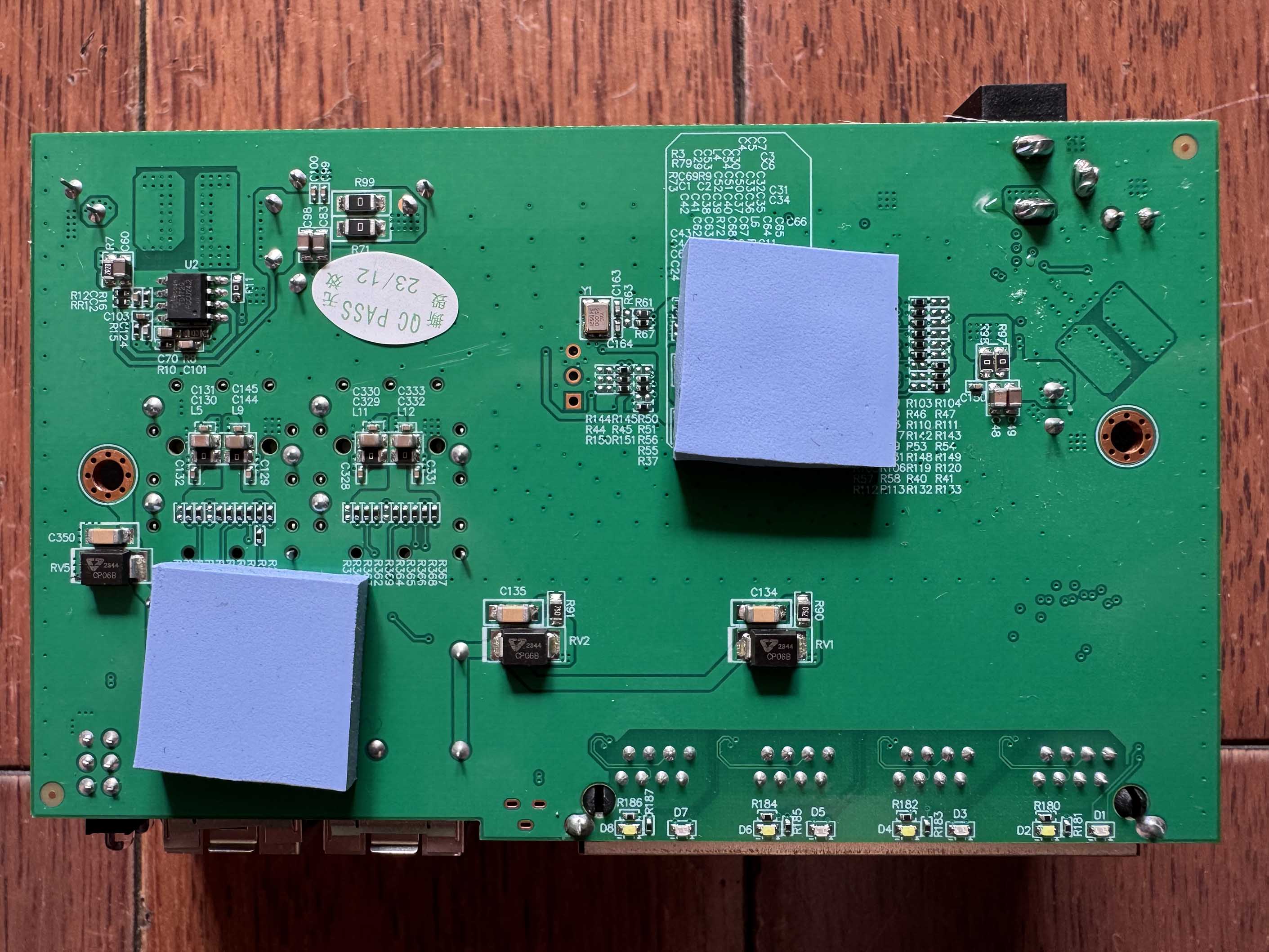
- The reset button footprint is unpopulated and the case has no opening for it,
so it could not be tested.
### PCB overview
**Board markings**
- Top silkscreen: `2G5F4_10G2_V1.01`
**Key components**
- Main switch: RTL8372 (RTL8371B family), reported as `RTL8372` (non-N) by
RTLPlayground. The chip sits under a heatsink and its package marking is not
readable.
- U1: SPI NOR flash, Bright Moon `T25S40`, 4 Mbit / 512 KB, SOP-8
- A 3-hole reset button footprint is present but unpopulated, and the case has
no opening for it, so there is no usable reset button
Top side:
 Bottom:
 The stock flash chip, Bright Moon `T25S40` (SOP-8, 4 Mbit / 512 KB):
 ### Port layout
| Front panel position | Logical port | Physical port | Type |
|----------------------|--------------|---------------|---------|
| SFP left | 8 | 5 | SFP+ |
| RJ45 1 | 4 | 1 | Copper |
| RJ45 2 | 5 | 2 | Copper |
| RJ45 3 | 6 | 3 | Copper |
| RJ45 4 | 7 | 4 | Copper |
| SFP right | 3 | 6 | SFP+ |
Copper ports 1–4 match the KP-9000-6XH-X2 (2M-PCB43-V1.1) layout, which this
board is a sibling of. The two SFP+ cages are wired the other way round
compared to that board: physical port 5 is on SDS1 and physical port 6 is on
SDS0.
### Serial console
The board has three through-holes used as the serial console. **The silkscreen
labels are wrong**: they are shifted relative to the actual signals.
| Silkscreen label | Actual signal |
|------------------|---------------|
| TX | GND |
| RX | TX |
| GND | RX |
Wiring (following the measured signals, not the labels):
| USB-TTL adapter | Board pad |
|-----------------|----------------------|
| GND | pad labelled `TX` |
| RX | pad labelled `RX` |
| TX | pad labelled `GND` |
- **Settings**: 115200 baud / 8N1 / 3.3V TTL (RTLPlayground), 9600 baud for the
stock firmware
- The stock firmware only prints a few bytes and a factory test menu
(`?`, `rst`, `f`, `r`, `10`, `100`, `g1`, `sd`, `eye`, …); it is not an
interactive management console
### LED configuration
Case silkscreen:
```
White : 2.5G
Blue : 1000M/2.5G L/A
```
| Port | LED | Linked, idle | With traffic |
|------------|--------------|--------------|--------------|
| Copper | white | 2.5G only | same |
| Copper | blue | solid | blinks (L/A) |
| SFP | single LED | solid | blinks (L/A) |
Measured LED-ID mapping (from the RTL837x LED set registers):
| LED-ID | Function |
|--------|---------------------------------|
| LED-ID0| copper blue LED |
| LED-ID1| copper white LED |
| LED-ID2| SFP single LED |
**Important**: `RTL837X_REG_LED_GLB_IO_EN` bit 6 must be set in
`machine_custom_init()`. Without it the RTL837x "solid" conditions (LINK/speed)
do not drive the LEDs at all and only `ACT` does, which makes the white LED
glow faintly at non-2.5G speeds.
### SFP GPIO assignments
| SFP | pin\_detect (ModAbs) | pin\_los | SerDes | I2C SDA | I2C SCL |
|-------------------|-------------------------------|------------------|--------|-------------------------|--------------------------|
| Left (logical 8, physical 5) | GPIO30\_ACL\_BIT3\_EN | GPIO37 | SDS1 | GPIO39\_I2C\_SDA4 | GPIO40\_I2C\_SCL3\_MDC1 |
| Right (logical 3, physical 6)| GPIO50\_I2C\_SCL2\_UART1\_TX | GPIO10\_LED10 | SDS0 | GPIO41\_I2C\_SDA3\_MDIO1 | GPIO40\_I2C\_SCL3\_MDC1 |
`pin_tx_disable` is GPIO\_NA on both ports. Both I2C buses are confirmed
working: with the same 10G module inserted, the `sfp` console command reads its
vendor and model from the left cage (`Slot 1`) and from the right cage
(`Slot 2`), DDM values included. The insertion also shows which SerDes drives
each cage - the left cage reports `sds_config sds: 01` and the right cage
`sds: 00`, which matches the table above.
### Machine target
Build for this device with `make MACHINE=2G5F4_10G2_V1_01`, which selects the
`machine/2G5F4_10G2_V1_01.c` board definition. It is derived from
`machine/KP_9000_6XHML_X2.c` with the SFP cage order and the reset pin changed.
The fitted T25S40 cannot be read in DIO mode on this board: an image that leaves
DIO enabled does not come up at all, both at the default read clock divider of 4
and at 8 (two boards tested), while the same image with single-IO boots and runs
normally. The board definition therefore sets `flash_sio`, which makes
`flash_init()` use `CMD_FREAD` at divider 8. Only the management plane is
slower, the ASIC keeps forwarding in hardware.